Low-temperature plasmas
The tailored wave
Boosting the efficiency of plasmas tenfold with the same energy input.
Plasmas are called the fourth state of matter: in the solid phase, their molecules occupy solid places, whereas there is some freedom of movement in the liquid phase and a lot of more freedom of movement in the gas phase. If more energy is supplied to a gas, the molecules break up and a plasma is created. The negatively charged electrons separate from the positively charged atomic nuclei and turn them into ions. These free electrons and ions can be accelerated by electromagnetic fields. If the fast electrons collide with other molecules, they can change them in turn by ionising or breaking them down. This process can result in different, sometimes short-lived reactive neutral particles and ions that may be useful for a variety of applications.
Smartphones, laptops, wafers
In the industry, plasmas are used, for example, to modify surfaces in a specific way, including coating spectacle lenses or displays or etching microscopic channels into silicon wafers. This results in fine structures in the nanometre range. “Every smartphone, every laptop contains components that have gone through such processes,” as Dr. Julian Schulze from the RUB Institute for Electrical Engineering and Plasma Technology outlines the use of plasmas in industrial applications. His aim is to better understand the details of processes in plasmas in order to render them more efficient. How is energy supplied to electrons and ions? How are they accelerated? How can this process be optimised?
In order to explore these questions, he concentrates on plasmas that are generated at room temperature, so-called low-temperature plasmas. They are often used for medical and industrial applications, because they do not damage or destroy their surrounding surfaces. In the medical field, this applies to e.g. human skin.
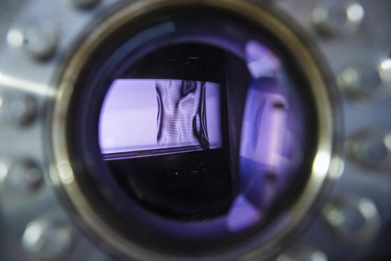
Such plasmas can, for example, be ignited between two electrodes, one of which is grounded, while a voltage is applied to the other. Applying the voltage leads to the generation of an electric field at the electrodes, which repels the negatively charged electrons from the surfaces while attracting positively charged ions. Because of the rapid movement of the electrons as a result of this acceleration, neutral particles can be excited by collisions with fast electrons. This ultimately makes plasmas glow. The acceleration of the ions to the surface can be used for surface modification.

Typically, a sinusoidal voltage is applied to the electrode – including industrial applications. This accelerates the electrons in a specific way. This, in turn, causes the plasma to emit light – which can be measured – at certain times and positions. Furthermore, positive ions reach the surfaces with a very specific energy distribution. However, Julian Schulze is not satisfied with this result: “Many electrons receive some of the energy that is fed in, but many of them do not receive enough to efficiently break up other molecules and, thus, produce high reactive particle densities. Also, the ion energy distribution at the interfaces cannot be controlled efficiently,” he points out. “We do not want to distribute the energy to electrons and ions with a watering can, but to deploy it in a more controlled manner so that fewer electrons receive more energy and the ion energy at interfaces can be precisely adjusted. This will enable plasmas to work more efficiently.”
The energy input to the electrons of the plasma can be controlled and improved
To this end, his team experimented with the form of the voltage waveform applied to the electrode and used in simulations. The process developed at RUB is called Voltage Waveform Tailoring, VWT for short. By superimposing several frequencies, different voltage waveforms can be generated, and the researchers have studied their effects on the plasma.
It emerged that, by tailoring this voltage waveform, the temporal and spatial distribution of the energy input to the electrons of the plasma can be controlled and improved. In the same way, the ion energy distribution at interfaces can be adjusted. “While in the case of the sinusoidal voltage many electrons are weakly accelerated at different points in time and over wide spatial areas, we have succeeded in using such optimised voltages to cause a much stronger acceleration of certain electrons at only one point in time within a period of the applied voltage and at specific spatial positions within the plasma,” explains Schulze. Thus, while the same amount of energy is dissipated, the amount of reactive species generated in the plasma increases. In principle, the situation is similar with ions: here, too, the acceleration of the charge carriers can be tailored with regard to time and space.

You have to imagine this in a similar way to when you pull a tablecloth away from under dishes so quickly that they simply remain where they were.
Julian Schulze
The mechanisms underlying these changes are the subject of in-depth studies. The effect of the voltage waveform on the plasma is rooted in the change in the relevant boundary zones near the electrodes, called plasma sheaths: the area in which a strong electric field exists, which is created by applying the voltage to the electrode, is a taboo zone for electrons; they are repelled. The positively charged, heavier, slower and colder ions, on the other hand, are attracted. The form of the applied voltage waveform modulates this boundary zone: it expands according to a pattern influenced by the voltage waveform and collapses again. “The electrons are kicked back into the plasma from the moving boundary region like a tennis ball from a racket,” as Julian Schulze illustrates one of several mechanisms that take place in the plasma. If the boundary layer is modulated so that it moves very fast, the electrons cannot keep up with it as quickly. “You have to imagine this in a similar way to when you pull a tablecloth away from under dishes so quickly that they simply remain where they were, even though you pull the floor away from beneath them. Then, you have to collect the dishes by hand, they do not follow the motion of the tablecloth,” says Schulze.

The positively charged ions perform the reverse motion, because they are accelerated towards the interfaces by the electric fields in the plasma boundary layer. Fast high-energy ions can be used to etch the interfaces, slower low-energy ions for coating. In any case, their energy and, thus, the processes on the surfaces can be tailored by VWT.
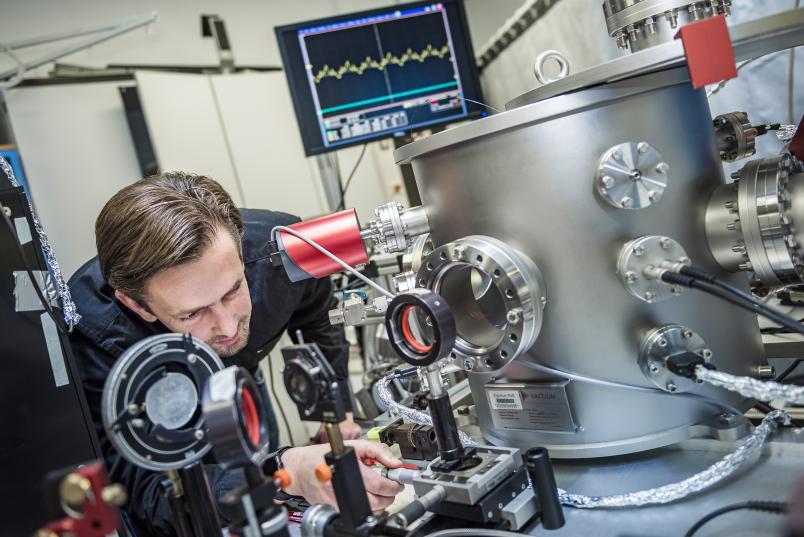
In order to find out exactly which mechanisms are at work when such tailored voltage waveforms are applied to the plasma, the engineers use e.g. high-resolution cameras to measure the electron dynamics. Moreover, laser measurements can be deployed to detect excited helium species and other reactive particles such as atomic oxygen, which are generated by collisions between neutral particles and energetic electrons. Since the excited helium particles absorb the laser radiation, it is possible to draw conclusions about the number of particles present by measuring the laser light that is transmitted by the plasma.
By superimposing two frequencies of the voltage applied to the electrode, the researchers measured a density of the particles that was more than five times greater. “Compared to applying the sinusoidal voltage, it is possible to increase the density of such particles tenfold and to control it by adjusting the voltage waveform,” Julian Schulze points out. Given the extent to which plasma is used in the semiconductor industry, the significance of this improvement is evident. “This is a billion-dollar industry,” says the researcher. “Every increase in efficiency has a huge economic impact.”


