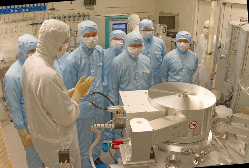
Japanese scientists in front of the unique cluster tool for 2D electronics at ForLab Bochum during the cleanroom tour.
The 17-member delegation visited the Ruhr-Universität on Monday, February 10, 2025.
The Japanese group also visited the Center for Interfacially Dominated High Performance Materials.
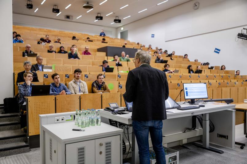
Günther Meschke, Vice-Rector for Research and Transfer, welcomed the delegation to the lecture hall.
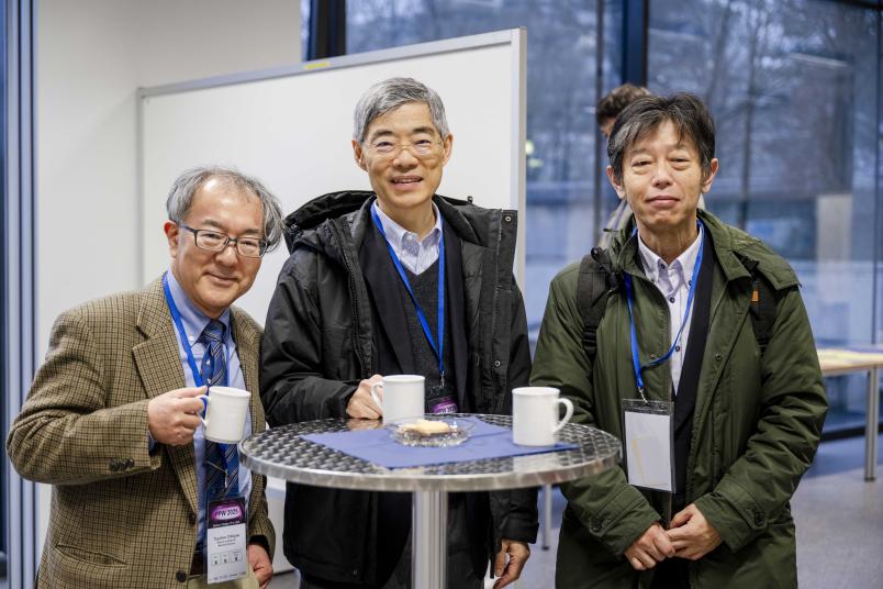
Relaxed break: Dr. Toyohiro Chikyow (National Institute for Materials Science), Prof. Dr. Akira Uedono (University of Tsukuba) and Dr. Hiori Kino (National Institute for Materials Science). Ruhr-Universität has been working with both institutions for a long time.
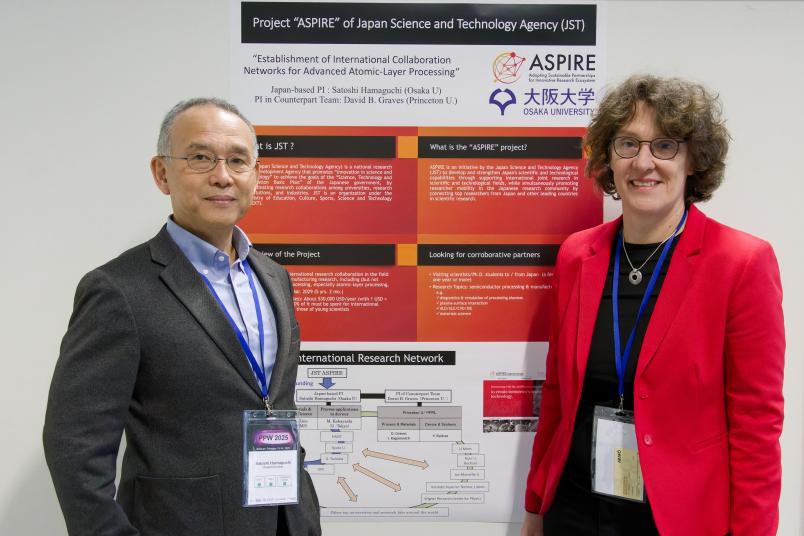
Prof. Satoshi Hamaguchi (Osaka University) and Dr. Claudia Bock (RUB) took the organization of the PPW 2025 workshop into their own hands. Here they stand in front of the poster on the Aspire program, which made the trip of the Japanese delegation possible.
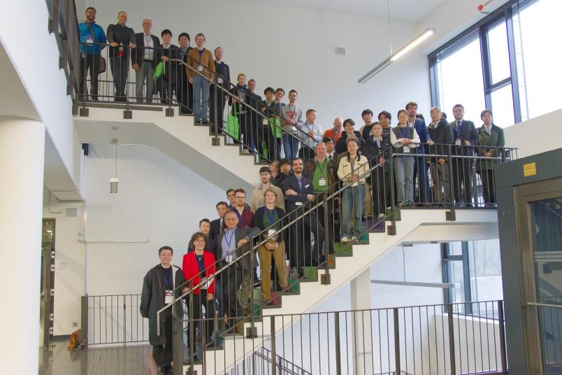
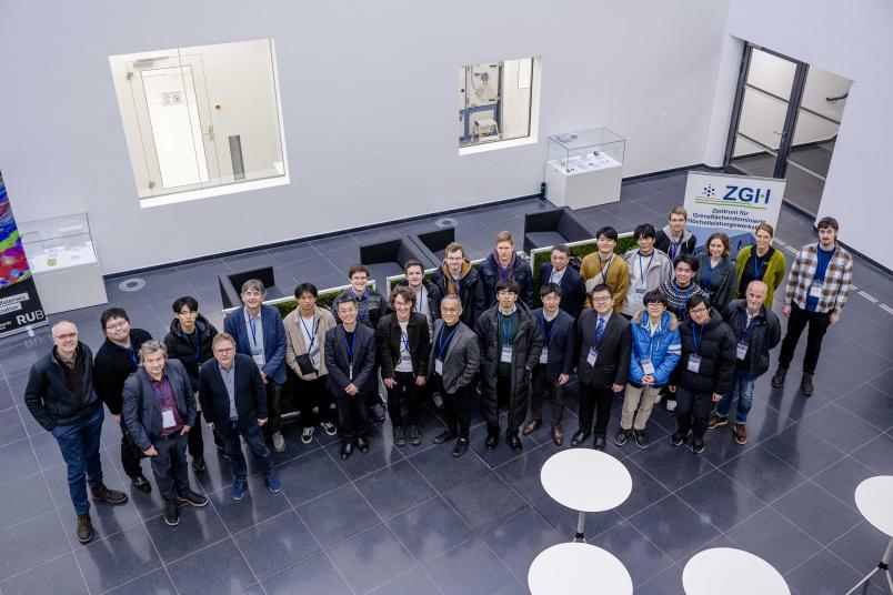
Group photo of the workshop participants
Internationalization
Customized Plasmas for Next Generation Microelectronics
An international cooperation aims to accelerate the transfer of research results into commercial applications in order to strengthen the microelectronics industry in Europe.
Global progress depends to a large extent on the ongoing evolution and unlimited availability of microelectronics – a technology that is indispensable in all areas of life and industry. The crises of recent years have shown that new alliances will be necessary to secure this key technology of the 21st century.
Ruhr University Bochum is part of an international network of Japanese, European and US partner institutions that are seeking to pioneer sophisticated semiconductor technology with atomic control for chip manufacturing. A cooperation to contribute to the implementation of the European and Japanese Chips Act was initiated at the 1st German Japanese Plasma Processing Workshop for Advanced Microelectronics in Bochum on February 13 and 14, 2025. A 17-member delegation from Japan visited Ruhr University Bochum as one of the top research institutions in this field. “An exchange with leading international plasma laboratories and experts in microelectronics production adds considerable value and can massively accelerate development processes in the context of the European Chips Act,” said Professor Günther Meschke, Vice Rector for Research and Transfer at Ruhr University Bochum.
Two-dimensional materials, i.e. materials that consist of only one or a few atomic layers, are gaining in importance in the production of computer chips. They are an integral part of global More than Moore strategies that involve more than just the ongoing development of silicon-based microelectronics. Plasmas are indispensable for producing them in a controlled manner and rendering them usable in technology. Ruhr University Bochum is researching the basic principles of these processes at ForLab Bochum as part of the 19 Research Laboratories Microelectronics Germany (forlab.tech) in close cooperation with the Center for Interfacial High Performance Materials and the Plasma and Materials Research Departments at Ruhr University. The aim is to translate findings from basic research into industrial applications at a faster pace. “Ruhr University of Bochum has long been known as one of the leading universities in the field of plasma science and recently started to apply its plasma technologies to 2D microelectronics device fabrication processes, which are now developed in the Forlab project called ‘Forschungslabor Mikroelektronik Bochum für 2D Elektronik’. Although plasma processes are widely used in the microelectronics industry, direct collaborative research between plasma science and advanced microelectronics device development is extremely rare and expected to lead to substantial innovation in future semiconductor manufacturing technologies. This interdisciplinary collaboration is of great interest to our ASPIRE project for microelectronics,” says Professor Satoshi Hamaguchi (University of Osaka, Aspire Coordinator and Mercator Fellow at Ruhr University Bochum).
The trip of the Japanese delegation is funded by the “Aspire” program of the “Japan Science and Technology Agency” to promote global exchange. The Aspire program is designed to initiate an international collaboration network, including mobility programs for young Japanese researchers. The sub-project “Establishment of International Collaboration Networks for Advanced Atomic-Layer Processing” will strengthen international collaboration between the plasma community and the microelectronics community.